- 已加入
- 2/25/10
- 訊息
- 393
- 互動分數
- 14
- 點數
- 18
- 年齡
- 45
I spent some time with new review of motherboards. And today we are continue in my motherboards passion  . Ussually people dont much like motherboards tests. It is weird and boring. But today we can try to show whats channged on Intel platforms after 10 years! How changed CPU performance with the same numbers of cores and threads??? Stand against 45nm CoreQuad Q8200 and 14nm++ Core i7-8086K. i7-8086 was configured as 4C/4T in BIOS. Generally for testing I used legacy tests. Maybe it could be more fair to Q8200.
1. introduction
It is around 10 years ago, when Core Quad 45nm was inducted. And Q8200 was popular and "cheap" variant of Q95xx models. The pricing politics was more friendly than today.
Core Quad 8200 has limitation in smaller L2 cache druhé against 9000 series, that Q8200 has 4MB of L2 (2x 2MB), but CPU had solid performance for the price point. The base clock is 2.33 GHz, but with overclocking you can reach between 3-3.3 GHz.
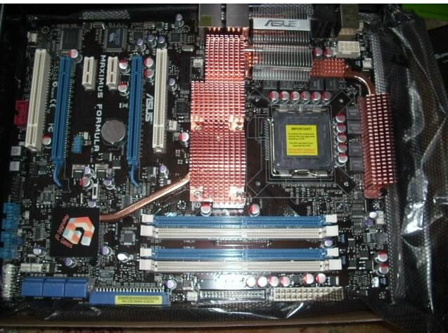
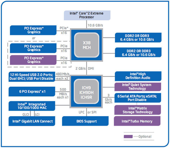
And what were good motherboards for it? One of the best was Maximus Formula chipset Intel X38. It is still class in motherboard world. Who would not remember with a little nostalgia for one of the first ROG boards? Maximus Formula is 11 years old. And X38 chipset had good equipment as you can see on screenshot. Of course, today is situation a little different...
Diagram of Intel X38 chipset
2. Maximus XI Apex in theoryi
The main goal and existence of the Apex board is extreme overclocking. In the market is more OC special boards (eg Maximus XI Gene and Extreme board has also special function for LN2 overclocking), but Apex is more ready for liquid nitrogen fun. There are special switches, sensors, layout...So specialized MBs is not much, currently I remmeber only EVGA Z390 Dark. Apex XI is third "Apex" in road, I remember 2017 year and first Maximus IX Apex as new king of overlcocking records.

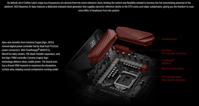
Motherboard has really strong VRM, downright extreme. CPU i9-9900K will have not limited in any situation. There are 2x 8-pins for better power distribution from PSU.

Interesting are individual temperature sensors. One is in the socket.
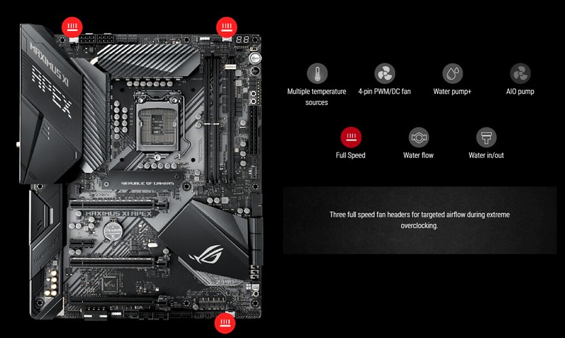
For extreme overlcocking people need special 4-pin connectors. These connectors spins without PC is powered on (need only 24-pin ATX) For extreme overcloking you need drain out all vapor.
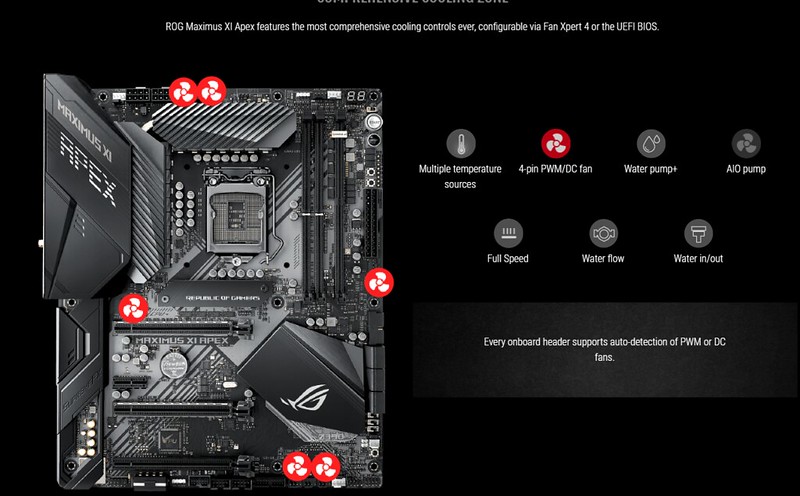
Another 6 next PWM connectors are classic PWM or DC for daily users Also, AIO PWM 4-pin is here as 7th connector on the motherboard!
Apex is unique also with support double capacity memory modules. Special DRAM modules are not cheap, but on Gene or Apex you cna use it and to have 64 GB capacity of RAM in two slots!

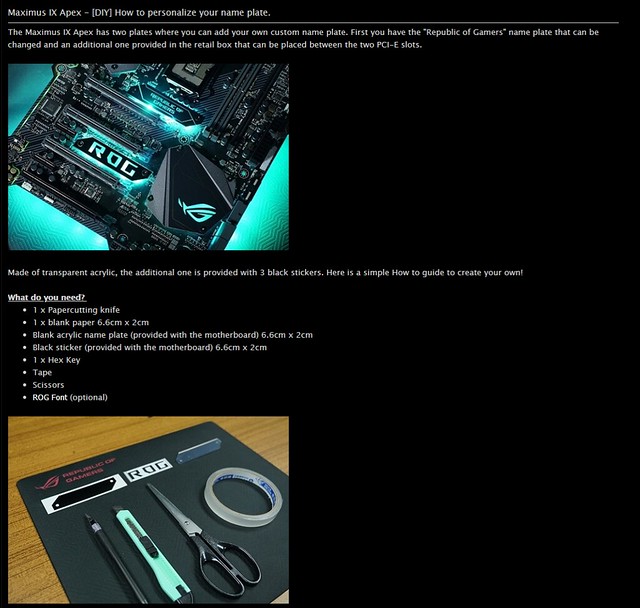
On the visual side, you can also customize the logo on the board to your own image. You can also find on ROG forum older instructions "How to do it".
Lets also look at another, rather hidden part, paired with the board software.

TPU function(and chip) is for intelligent OC tweaking of your PC. At Asus Z390 boards you propably know special function of OC prediction function* - depends on your actual cooling system and temperature changes as results PC winter/summer/dust in cooler etc. This is cool function, right?
*this function must be enabled in BIOS settings and also for real time prediction as "keep training" value

This part of the fan control and the airflow in the PC case is my favorite. I've been using it for years and it works well. Today is as version FanXpert4.
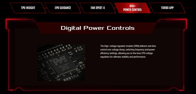
Digi+ Control focused on VRM settings. More experience guys can set everything manually in BIOS, but it is still good to have in Windows and software. ROG Z390 boards and LLC settings - best way for load is LLC7.
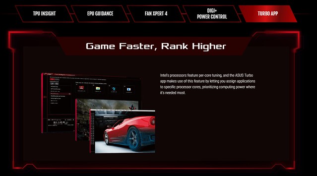
The Turbo application is related to the fact that Intel allows you to set each CPU core separately in frequency. And this can be useful for various applications where you define how many cores the application should use and at what frequency.
3. Motherboard - Outputs, connectors and VRM diagram
The box is in the traditional ROG jacket as we know it for years. On the back of the box we see the main points that the board offers.

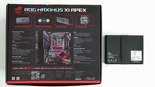
Itself board peeks inside and then the accessories placed separately in the miniboxes
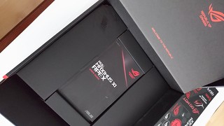


- accessories include lots of ROG stickers, WiFi antennas, M2 screws, coaster, SATA cables, massive DIMM M2 card, HB SLI bridge, braiding cables discount coupon, RGB extensions and nickname plate.
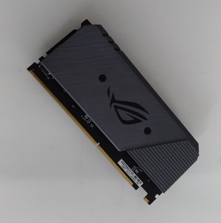
DIMM M2 card. Under the massive aluminum cooler is the PCB of card and the possible two-sided attachment of M2 discs. The M2 storages will be great cooled and the performance will not drop even under load.


The motherboard looks beautiful. Is it not more X PCB design here, but in the colors design is imaginary "X" still there. Motherboard is in black and gray colors. Massive board VRM cooler dominated there and there are a lot of function buttons and switches. The connectors are in common places, but the connector power for the processor is doubled (2x 8-pin)

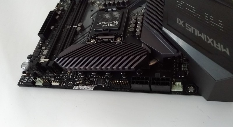
-detail on the front of a massive aluminum passive that hides the powermosfets. White 4-pins are for fans that run at full speed even when the PC is off (they are only 24-pin dependent). We also see the Digi + control ASP1405 chip for processor power phase.
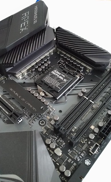
There are huge VRM of board under the massive cooler. As you will see later, it is really massive and oversized - so it is supposed to look on the enthusiastic boards
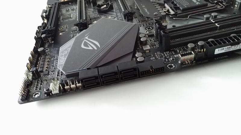
The bottom right corner of the board offers six SATA. To them to the right are the front USB 3.0 and USB3.1. To the left of SATA are switches designed for extreme overclocking with liquid nitrogen. It is a switch "pause", "slowmod" and "RSVD". The pause is for the actual bench pause while you are running - you can cool down the processor in the meantime and then continue the test. Slow Mode is for safe low-frequency boot or saving result image after high clocks benchamrking/validation process. And RSVD switch prevents coldbug-enhancing processor and system behavior at heavily negative liquidfnitrogen cooling temperatures.
We also see the small jumper "LN2" that opens some of the high voltage values in the BIOS and then the white special connectors for water cooling.
The board has two BIOSes, so one button is the last one on the left. BIOS switching is indicated by a diode on the BIOS chip.
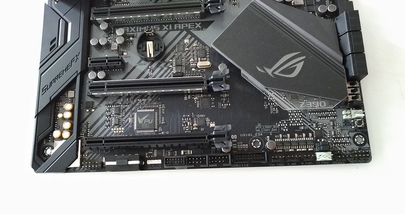
Bottom edge of the board from left to right: audio connector, additional power supply connector for PCIe slots if you use multiple graphics cards, programmable RGB header, special NODE connector and 2x USB2.0 header and 1x USB3.0 header. Then 4x four-pin PWM connectors of different design (classic, 3A for powerful fans, for water pump and white for full operation at 100% speed even when connected to a PC). Finally, there are two sensor connectors and connectors for the PC case.
-Also note the two jumpers for the board RGB section
-above the bottom long PCIe slot is a large TPU control chip for communication through Ai Suite III software.
At this photo is the main IO chip NCT6798D for monitoring and control of example fan speed.

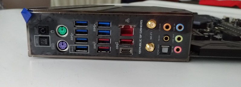
The rear outputs are already on the integrated IO panel. This will facilitate installation in a PC case. There are buttons for clear the BIOS, BIOS flashback button, PS2 for mouse and keyboard - this is very useful for extreme overclocking and older operating systems. Furthermore, 6x USB3.0, 2x USB3.1 and other USB3.1 + USB3.1 type C. And of course an RJ45 connector with antisurge protection, dual wifi (2.4/5GHz) outputs for antenna (included) and audio outputs with 8.1 sound support.
This is how the motherboard looks after unscrewing the covers and the coolers themselves.

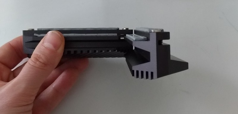
passives have heat conducting tapes for cooling mosfets and coils, it is well profiled.
How voltage regulator communicate at Z390 Asus and how is difference software vs. real voltage on Asus Z390 (And so does the same at Crosshair VII Hero X470 AMD) explains ex-engineer of Asus ROG division in this post, which I dared to insert in the form of an image.
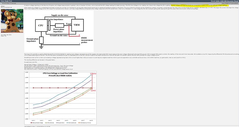
[highlight=yellow]VRM schema and description[/highlight]

I marked the power supply connectors of the board in green (I forgot to frame the bottom PCIe additional power of the slots) 24-pin and 2x 8pin
In orange, I framed the PCIe slots and directed the arrows to communicate with the South Bridge or CPU. The very bottom is the four-speed PCIe 3.0. The rest are PCIe x8 3.0 and PCIe x16 3.0. Then we see only one short PCIe x1 slot.
White frames belong to three special connectors for fans, where the connected fans run even when the PC is off (24-ATX connector required)
The processor cores are made up of a total of 16 phases over doublers. In other words, the true eight-phase VRM. I highlighted it all in red. Pink color is main controller of this phase - ASP1405 and next pink frame as special chip for precise CPU software Voltage Detection (in CPUZ, hwinfo etc.)
The blue area includes two memory-phases, digitally controlled. Then their control chip marked as pink.
The yellow color is then the simple phases for the IO and the SA part of the processor.
CPU VRM part
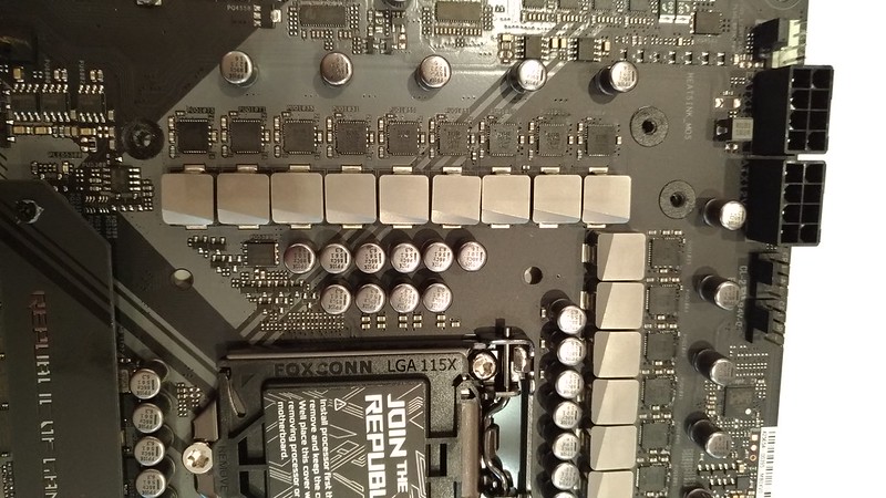
I have already mentioned that the new Apex has sixteen pahses for the processor. It is also interesting to note that Apex has no phases delimited for iGPU. Therefore, this board really counts just for CPU world records. The main controller is labeled as ASP1405, the powerpack mosfets contain classically upper and lower mosfet plus driver. But it is inside the pack :). The complete mosfet complex is very good IR3555M. One phase can deliver up to 60A in normal conditions. That is, just for processor of an unbelievable 960A !
Here we see the detail of the DRAM power phase + few function buttons. Above the start and reset buttons there is a switch for the MEM OK II function. After a few unsuccessful attempts (I think three times) and the memory settings will return you automatically to the BIOS with a safe setting to change the item in the DRAM timings. There is also a jumper near the switch to activate or deactivate the light effects of the board.
To the right of the 24 ATX connector are the "Retry" and "safe" OC buttons, which are also useful. Retry will try to stand up and boot with the setting it failed the first time ideal when you turn off the MEM OK II switch, because sometimes more than 3 posts are needed to successfully boot) [/ i]. A safe button will return you to the BIOS after an unsuccessful attempt without deleting previous BIOS values. These are especially useful for overclockers. And also on the edge of the board we see the voltage measuring points.
DRAM VRM is based on digital controller ASP1103, two chokes R33 and for mosfets (I can not read mosfet with my eyes )

4. BIOS for geeks and test methodology
BIOS has been known for years, similar to previous ROG Apex, very detailed and with several keyboard shortcuts to invoke various submenus or favorites. Interesting is the prediction of overclocking with normal cooling systems
For fanatics I have BIOS screenshots to download: TBD (later)
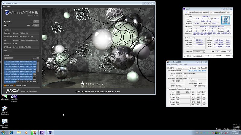
I used the following as test kits:
ROG Maximus XI Apex
Core i7-8086K "downsize" at 4C/4T processor
cooling AIO ROG Ryujin 360
RAM 2x 8GB GSkill TridentZ Royal 4000 MHz
GPU ROG Strix GTX 1050 OC 2GB
PSU Corsair AX1200
SSD HyperX 120 GB

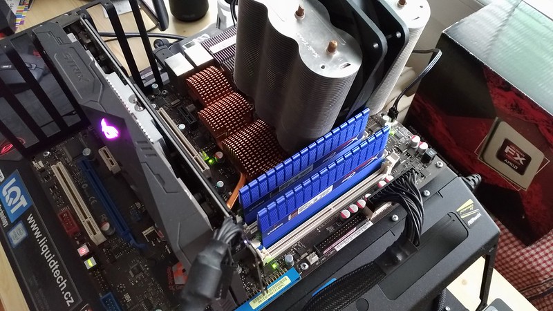
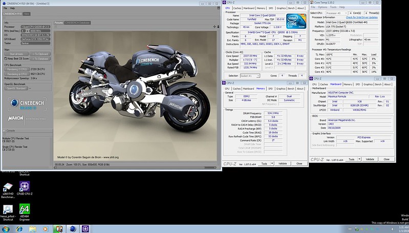
ROG Maximus Formula
Core Quad Q8200
cooling ThermalTake Sonic Tower + active fan
RAM 2x 2GB HyperX 1066 MHz
ROG Strix GTX 1050 OC 2GB
PSU Corsair AX1200
SSD HyperX 120 GB
5. Test results in graphs
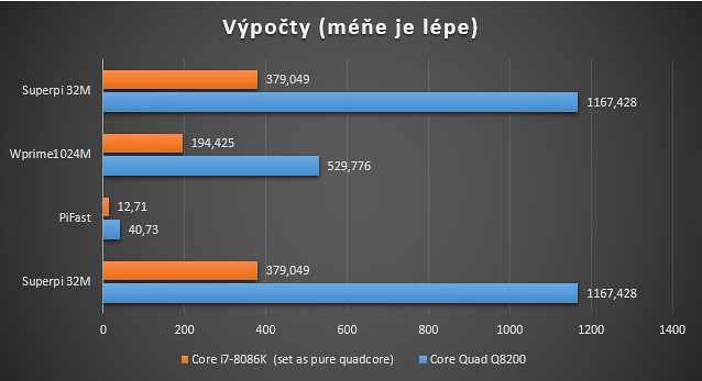
For an overview, I put the results of both CPUs in graphs.
Computing operations are in seconds, lower means better (Superpi on 32M, PiFast and more modern wprime 1024M)
Fritczhess is chess CPU computing with support of up to 16 threads. Higher score is better.

Working with DRAM includes the AIDA64 subtest. The values are in MB / s
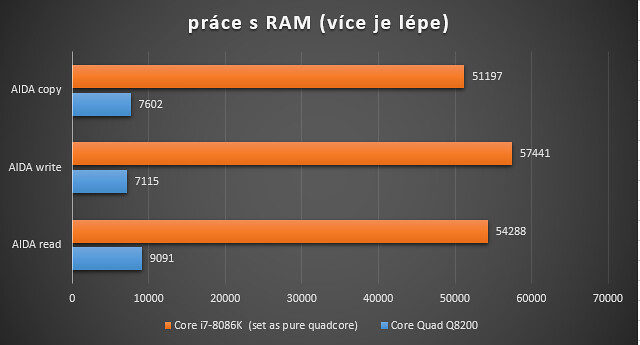
Rendering was used ten years ago and is still in use today. I have included three generations of Cinebench, where the oldest one is used to compare the clear performance of one core (CinebenchR10), the other two are using all cores. And that Superpi got in the graph there by mistake

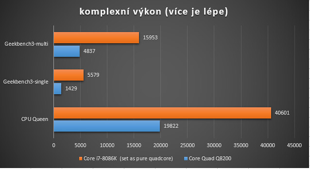
Complex performance is represented by Geekbench3. Incredibly, slightly older Geekbench3 seems to be a better performance comparison method than the last Geekbench4. This is especially true for subtests (eg RAM subtests, etc.) AIDA64 as CPU Queen universal quick test. More points are better.
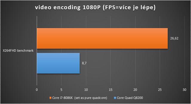
The FHD video encoding was the absolute maximum 10 years ago, today it is a common standard. The x264 codec is still very popular. And of course the higher value of FPS is better.
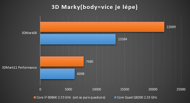
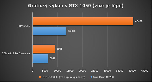
What about graphic subtests? Today, the GTX 1050 is still usable card on FHD resolution. It will be interesting in the less demanding 3DMark06 and more challenging 3D Mark11 on both platforms.
6. How much jumped the performance in those generations? And what about Maximus XI Apex?
The results of the measurements are over and let's summarize them. With the same number of cores, the result in Superpi is one-third the time, which is a huge leap (of course, the lion's share of it is processor frequency - 2.33 GHz vs 4.7 GHz during this test). Multithreaded wprime more than double the performance for i7-8086K 4C/4T.
In single thread CinebenchR10 is performance almost quadruple. Working with RAM has progressed leaps and bounds.
Mostly the performance with the same number of cores has improved by more than twice as much as four times. It is necessary to state that the performance of the processors is growing, although it does not always look so unambiguously in the inter-generational context.
Also interesting is the result of 3D Marks. While 3DMark11 has a higher resolution than 3DMark06, the GTX 1050 is not so much in it. 3DMark06 is then more dependent on the processor and suddenly the edge of a modern processor is triple in this graphical test

i7-8086K 4C / 4T CPU boosted to 4.3 GHz at full load
While the Core Quad Q8200 only at 2.33 GHz. And this is actually a 2 GHz difference. So we can say that the frequencie in those 10 years on similar Intel architectural basics has jumped a nice 2 GHz up. If the Q8200 went overclocking to say 3.3 GHz, which is a very high jump, then today's i7-8086K goes from 4.3 GHz turbo, say at 5 GHz. That is also not enough, but at that time the relative jump in performance due to overclocking was higher!
In basic, the big difference of base clocks was one of main keypoints of performance results in this fight. Also some of the computational instructions (in CinebenchR15, X264FHD), but also the communicate of the memory controller and the communication of individual cores among themselves (much visible in AIDA throughput), as well as the existence of L3 cache in modern Intel CPU. Such an upgrade from Core Quad to Core 8th or 9th Generation (but actually 7th) will be noticeable (or AMD of course). I subjected myself to great differences. On the other hand, for occasional gaming or web and movies, CoreQuad still does a good job.
What about the boards? The Maximus Formula was great, at the time with 6 USB ports on the rear output, dual LAN, optical output and input, SupremeFX dedicated audio card, curved SATA connectors, decent VRM with direct mosfet cooling and good ribbing. It had functional buttons for start, reset, CMOS reset and external post display, high qaulity caps where you look, one PWM connector (the remaining were DC controlled). Ability to save two OC profiles in BIOS. It just wasn't commonplace in 2008 ... The FSB limit was also high above 450 MHz. Today it is a beautiful piece of hardware in my collection. ...It is time to replace the old with a new one.
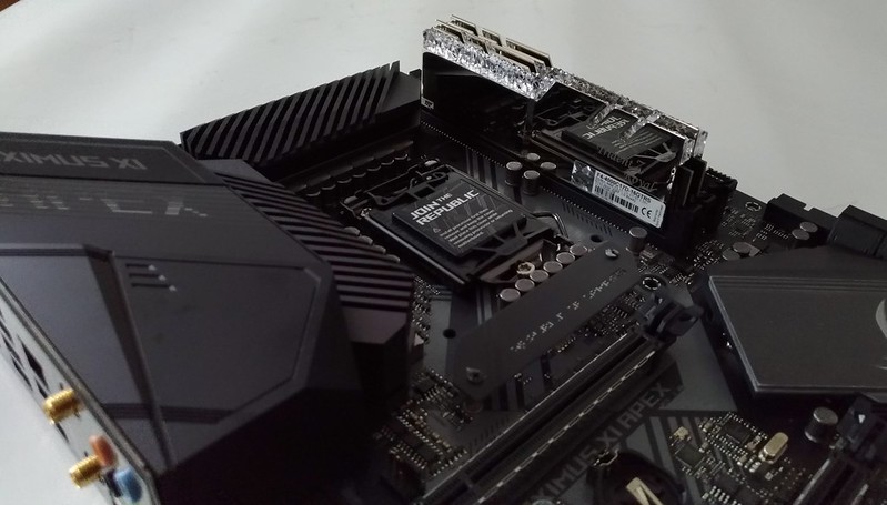
Maximus XI Apex is the highlight of today's enthusiastic offer along with the Extreme version. Everything works precisely, even there is a function for failed RAM post, which automatically throws us through bad memory training into the BIOS. I think there was an inspiration from AMD boards, where is this function on Ryzens (after 3 unsuccessful attempts it is suitable for default safe settings). Great for us - users. In BIOS you can find many OC profiles for CPU overlcocking and for memory special settings.
You can even use the BIOS settings like Tweakers paradise to set hours, even days, or manually set the memory itself. The board is absolutely accurate in voltage stability (LLC6 / 7/8), and no active VRM cooling is needed
1. introduction
It is around 10 years ago, when Core Quad 45nm was inducted. And Q8200 was popular and "cheap" variant of Q95xx models. The pricing politics was more friendly than today.
Core Quad 8200 has limitation in smaller L2 cache druhé against 9000 series, that Q8200 has 4MB of L2 (2x 2MB), but CPU had solid performance for the price point. The base clock is 2.33 GHz, but with overclocking you can reach between 3-3.3 GHz.

And what were good motherboards for it? One of the best was Maximus Formula chipset Intel X38. It is still class in motherboard world. Who would not remember with a little nostalgia for one of the first ROG boards? Maximus Formula is 11 years old. And X38 chipset had good equipment as you can see on screenshot. Of course, today is situation a little different...
Diagram of Intel X38 chipset

2. Maximus XI Apex in theoryi
The main goal and existence of the Apex board is extreme overclocking. In the market is more OC special boards (eg Maximus XI Gene and Extreme board has also special function for LN2 overclocking), but Apex is more ready for liquid nitrogen fun. There are special switches, sensors, layout...So specialized MBs is not much, currently I remmeber only EVGA Z390 Dark. Apex XI is third "Apex" in road, I remember 2017 year and first Maximus IX Apex as new king of overlcocking records.


Motherboard has really strong VRM, downright extreme. CPU i9-9900K will have not limited in any situation. There are 2x 8-pins for better power distribution from PSU.

Interesting are individual temperature sensors. One is in the socket.

For extreme overlcocking people need special 4-pin connectors. These connectors spins without PC is powered on (need only 24-pin ATX) For extreme overcloking you need drain out all vapor.

Another 6 next PWM connectors are classic PWM or DC for daily users
Apex is unique also with support double capacity memory modules. Special DRAM modules are not cheap, but on Gene or Apex you cna use it and to have 64 GB capacity of RAM in two slots!


On the visual side, you can also customize the logo on the board to your own image. You can also find on ROG forum older instructions "How to do it".
Lets also look at another, rather hidden part, paired with the board software.

TPU function(and chip) is for intelligent OC tweaking of your PC. At Asus Z390 boards you propably know special function of OC prediction function* - depends on your actual cooling system and temperature changes as results PC winter/summer/dust in cooler etc. This is cool function, right?
*this function must be enabled in BIOS settings and also for real time prediction as "keep training" value

This part of the fan control and the airflow in the PC case is my favorite. I've been using it for years and it works well. Today is as version FanXpert4.

Digi+ Control focused on VRM settings. More experience guys can set everything manually in BIOS, but it is still good to have in Windows and software. ROG Z390 boards and LLC settings - best way for load is LLC7.

The Turbo application is related to the fact that Intel allows you to set each CPU core separately in frequency. And this can be useful for various applications where you define how many cores the application should use and at what frequency.
3. Motherboard - Outputs, connectors and VRM diagram
The box is in the traditional ROG jacket as we know it for years. On the back of the box we see the main points that the board offers.


Itself board peeks inside and then the accessories placed separately in the miniboxes


- accessories include lots of ROG stickers, WiFi antennas, M2 screws, coaster, SATA cables, massive DIMM M2 card, HB SLI bridge, braiding cables discount coupon, RGB extensions and nickname plate.
DIMM M2 card. Under the massive aluminum cooler is the PCB of card and the possible two-sided attachment of M2 discs. The M2 storages will be great cooled and the performance will not drop even under load.


The motherboard looks beautiful. Is it not more X PCB design here, but in the colors design is imaginary "X" still there. Motherboard is in black and gray colors. Massive board VRM cooler dominated there and there are a lot of function buttons and switches. The connectors are in common places, but the connector power for the processor is doubled (2x 8-pin)


-detail on the front of a massive aluminum passive that hides the powermosfets. White 4-pins are for fans that run at full speed even when the PC is off (they are only 24-pin dependent). We also see the Digi + control ASP1405 chip for processor power phase.
There are huge VRM of board under the massive cooler. As you will see later, it is really massive and oversized - so it is supposed to look on the enthusiastic boards

The bottom right corner of the board offers six SATA. To them to the right are the front USB 3.0 and USB3.1. To the left of SATA are switches designed for extreme overclocking with liquid nitrogen. It is a switch "pause", "slowmod" and "RSVD". The pause is for the actual bench pause while you are running - you can cool down the processor in the meantime and then continue the test. Slow Mode is for safe low-frequency boot or saving result image after high clocks benchamrking/validation process. And RSVD switch prevents coldbug-enhancing processor and system behavior at heavily negative liquidfnitrogen cooling temperatures.
We also see the small jumper "LN2" that opens some of the high voltage values in the BIOS and then the white special connectors for water cooling.
The board has two BIOSes, so one button is the last one on the left. BIOS switching is indicated by a diode on the BIOS chip.

Bottom edge of the board from left to right: audio connector, additional power supply connector for PCIe slots if you use multiple graphics cards, programmable RGB header, special NODE connector and 2x USB2.0 header and 1x USB3.0 header. Then 4x four-pin PWM connectors of different design (classic, 3A for powerful fans, for water pump and white for full operation at 100% speed even when connected to a PC). Finally, there are two sensor connectors and connectors for the PC case.

-Also note the two jumpers for the board RGB section
-above the bottom long PCIe slot is a large TPU control chip for communication through Ai Suite III software.
At this photo is the main IO chip NCT6798D for monitoring and control of example fan speed.

The rear outputs are already on the integrated IO panel. This will facilitate installation in a PC case. There are buttons for clear the BIOS, BIOS flashback button, PS2 for mouse and keyboard - this is very useful for extreme overclocking and older operating systems. Furthermore, 6x USB3.0, 2x USB3.1 and other USB3.1 + USB3.1 type C. And of course an RJ45 connector with antisurge protection, dual wifi (2.4/5GHz) outputs for antenna (included) and audio outputs with 8.1 sound support.

This is how the motherboard looks after unscrewing the covers and the coolers themselves.


passives have heat conducting tapes for cooling mosfets and coils, it is well profiled.
How voltage regulator communicate at Z390 Asus and how is difference software vs. real voltage on Asus Z390 (And so does the same at Crosshair VII Hero X470 AMD) explains ex-engineer of Asus ROG division in this post, which I dared to insert in the form of an image.

[highlight=yellow]VRM schema and description[/highlight]

I marked the power supply connectors of the board in green (I forgot to frame the bottom PCIe additional power of the slots) 24-pin and 2x 8pin
In orange, I framed the PCIe slots and directed the arrows to communicate with the South Bridge or CPU. The very bottom is the four-speed PCIe 3.0. The rest are PCIe x8 3.0 and PCIe x16 3.0. Then we see only one short PCIe x1 slot.
White frames belong to three special connectors for fans, where the connected fans run even when the PC is off (24-ATX connector required)
The processor cores are made up of a total of 16 phases over doublers. In other words, the true eight-phase VRM. I highlighted it all in red. Pink color is main controller of this phase - ASP1405 and next pink frame as special chip for precise CPU software Voltage Detection (in CPUZ, hwinfo etc.)
The blue area includes two memory-phases, digitally controlled. Then their control chip marked as pink.
The yellow color is then the simple phases for the IO and the SA part of the processor.
CPU VRM part

I have already mentioned that the new Apex has sixteen pahses for the processor. It is also interesting to note that Apex has no phases delimited for iGPU. Therefore, this board really counts just for CPU world records. The main controller is labeled as ASP1405, the powerpack mosfets contain classically upper and lower mosfet plus driver. But it is inside the pack :). The complete mosfet complex is very good IR3555M. One phase can deliver up to 60A in normal conditions. That is, just for processor of an unbelievable 960A !
Here we see the detail of the DRAM power phase + few function buttons. Above the start and reset buttons there is a switch for the MEM OK II function. After a few unsuccessful attempts (I think three times) and the memory settings will return you automatically to the BIOS with a safe setting to change the item in the DRAM timings. There is also a jumper near the switch to activate or deactivate the light effects of the board.
To the right of the 24 ATX connector are the "Retry" and "safe" OC buttons, which are also useful. Retry will try to stand up and boot with the setting it failed the first time ideal when you turn off the MEM OK II switch, because sometimes more than 3 posts are needed to successfully boot) [/ i]. A safe button will return you to the BIOS after an unsuccessful attempt without deleting previous BIOS values. These are especially useful for overclockers. And also on the edge of the board we see the voltage measuring points.
DRAM VRM is based on digital controller ASP1103, two chokes R33 and for mosfets (I can not read mosfet with my eyes )

4. BIOS for geeks and test methodology
BIOS has been known for years, similar to previous ROG Apex, very detailed and with several keyboard shortcuts to invoke various submenus or favorites. Interesting is the prediction of overclocking with normal cooling systems
For fanatics I have BIOS screenshots to download: TBD (later)
I used the following as test kits:
ROG Maximus XI Apex
Core i7-8086K "downsize" at 4C/4T processor
cooling AIO ROG Ryujin 360
RAM 2x 8GB GSkill TridentZ Royal 4000 MHz
GPU ROG Strix GTX 1050 OC 2GB
PSU Corsair AX1200
SSD HyperX 120 GB


ROG Maximus Formula
Core Quad Q8200
cooling ThermalTake Sonic Tower + active fan
RAM 2x 2GB HyperX 1066 MHz
ROG Strix GTX 1050 OC 2GB
PSU Corsair AX1200
SSD HyperX 120 GB


5. Test results in graphs
For an overview, I put the results of both CPUs in graphs.
Computing operations are in seconds, lower means better (Superpi on 32M, PiFast and more modern wprime 1024M)

Fritczhess is chess CPU computing with support of up to 16 threads. Higher score is better.

Working with DRAM includes the AIDA64 subtest. The values are in MB / s

Rendering was used ten years ago and is still in use today. I have included three generations of Cinebench, where the oldest one is used to compare the clear performance of one core (CinebenchR10), the other two are using all cores. And that Superpi got in the graph there by mistake

Complex performance is represented by Geekbench3. Incredibly, slightly older Geekbench3 seems to be a better performance comparison method than the last Geekbench4. This is especially true for subtests (eg RAM subtests, etc.) AIDA64 as CPU Queen universal quick test. More points are better.

The FHD video encoding was the absolute maximum 10 years ago, today it is a common standard. The x264 codec is still very popular. And of course the higher value of FPS is better.

What about graphic subtests? Today, the GTX 1050 is still usable card on FHD resolution. It will be interesting in the less demanding 3DMark06 and more challenging 3D Mark11 on both platforms.

6. How much jumped the performance in those generations? And what about Maximus XI Apex?
The results of the measurements are over and let's summarize them. With the same number of cores, the result in Superpi is one-third the time, which is a huge leap (of course, the lion's share of it is processor frequency - 2.33 GHz vs 4.7 GHz during this test). Multithreaded wprime more than double the performance for i7-8086K 4C/4T.
In single thread CinebenchR10 is performance almost quadruple. Working with RAM has progressed leaps and bounds.
Mostly the performance with the same number of cores has improved by more than twice as much as four times. It is necessary to state that the performance of the processors is growing, although it does not always look so unambiguously in the inter-generational context.
Also interesting is the result of 3D Marks. While 3DMark11 has a higher resolution than 3DMark06, the GTX 1050 is not so much in it. 3DMark06 is then more dependent on the processor and suddenly the edge of a modern processor is triple in this graphical test

i7-8086K 4C / 4T CPU boosted to 4.3 GHz at full load
While the Core Quad Q8200 only at 2.33 GHz. And this is actually a 2 GHz difference. So we can say that the frequencie in those 10 years on similar Intel architectural basics has jumped a nice 2 GHz up. If the Q8200 went overclocking to say 3.3 GHz, which is a very high jump, then today's i7-8086K goes from 4.3 GHz turbo, say at 5 GHz. That is also not enough, but at that time the relative jump in performance due to overclocking was higher!
In basic, the big difference of base clocks was one of main keypoints of performance results in this fight. Also some of the computational instructions (in CinebenchR15, X264FHD), but also the communicate of the memory controller and the communication of individual cores among themselves (much visible in AIDA throughput), as well as the existence of L3 cache in modern Intel CPU. Such an upgrade from Core Quad to Core 8th or 9th Generation (but actually 7th) will be noticeable (or AMD of course). I subjected myself to great differences. On the other hand, for occasional gaming or web and movies, CoreQuad still does a good job.
What about the boards? The Maximus Formula was great, at the time with 6 USB ports on the rear output, dual LAN, optical output and input, SupremeFX dedicated audio card, curved SATA connectors, decent VRM with direct mosfet cooling and good ribbing. It had functional buttons for start, reset, CMOS reset and external post display, high qaulity caps where you look, one PWM connector (the remaining were DC controlled). Ability to save two OC profiles in BIOS. It just wasn't commonplace in 2008 ... The FSB limit was also high above 450 MHz. Today it is a beautiful piece of hardware in my collection. ...It is time to replace the old with a new one.

Maximus XI Apex is the highlight of today's enthusiastic offer along with the Extreme version. Everything works precisely, even there is a function for failed RAM post, which automatically throws us through bad memory training into the BIOS. I think there was an inspiration from AMD boards, where is this function on Ryzens (after 3 unsuccessful attempts it is suitable for default safe settings). Great for us - users. In BIOS you can find many OC profiles for CPU overlcocking and for memory special settings.
You can even use the BIOS settings like Tweakers paradise to set hours, even days, or manually set the memory itself. The board is absolutely accurate in voltage stability (LLC6 / 7/8), and no active VRM cooling is needed


